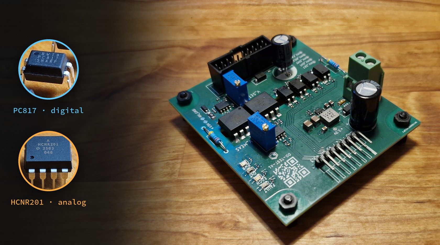
Sometimes you need to control and measure a voltage in a separate, isolated domain, with your microcontroller's GPIO/DAC/ADC while keeping the low-voltage side completely separated, to avoid ground loops or interference that could damage the sensitive electronics. One way to achieve this is to take the optical route and get the signals across with optocouplers.
This is something practical that I use in one of my developments (for testing purposes), and I find the whole concept quite interesting. I think it is worth going into more detail here and sharing how such a circuit works and how it can be built and used.
First things first: the two parts that make the optical isolation possible are the PC817 and the HCNR201. The PC817 is a generic optocoupler for transmitting digital signals. The HCNR201 is more interesting: it has a second photodiode on the input side that can be used to close a feedback loop. With it, the LED current is regulated so that the output voltage is linearly proportional to the input voltage. Two HCNR201s make it possible to both set and measure a voltage across the barrier.
Digital signals
Getting a simple digital signal across the isolation barrier is as simple as using a transistor. In fact, that is exactly what the PC817 is: a phototransistor whose base is driven by the light of the LED. The transfer is not precise, so it is only usable for ON/OFF states.
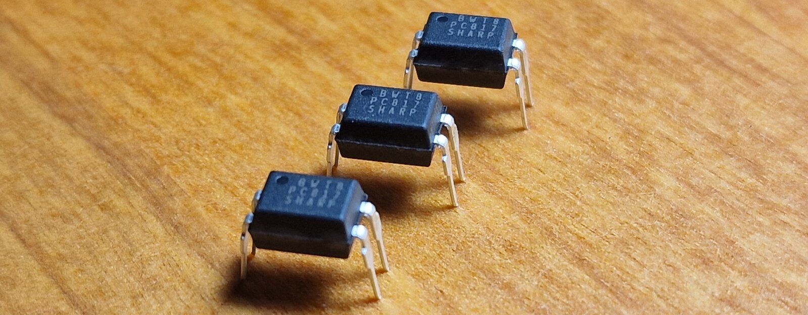
Let's say we want to read the state of a signal that is pulled to GND when a fault occurs. The input side is driven like a normal LED: a pull-up resistor goes to the supply on the high-voltage side, and when the fault signal pulls to GND, the LED lights up. On the low-voltage side, the collector is pulled to GND while the LED is lit.
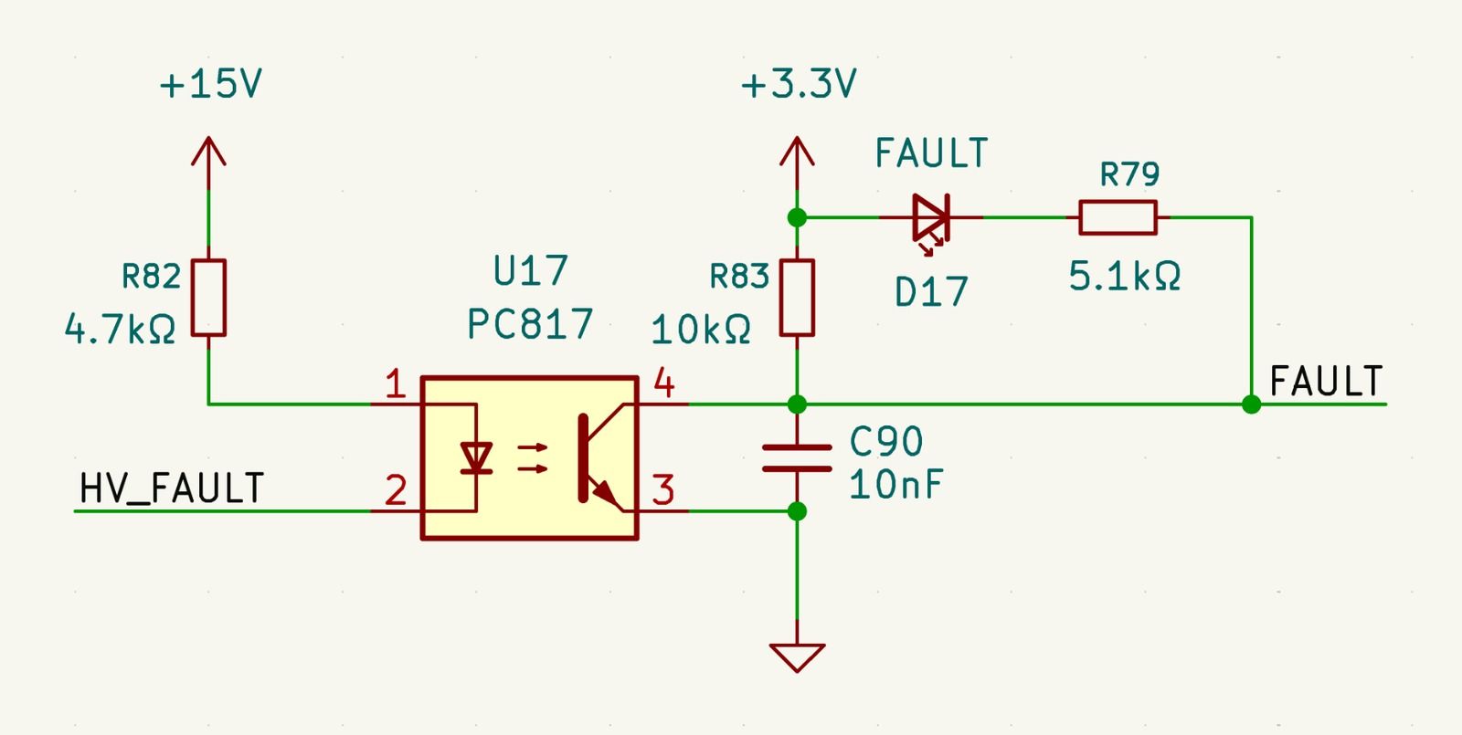
Here is how the values in this circuit are chosen:
- LED side (high-voltage domain). The fault output of the device I am reading is a bare open drain, so the board has to provide the pull-up: +15 V → R82 4.7 kΩ → LED → fault pin. When the pin pulls low, the LED current is I_F ≈ (15 V − 1.2 V) / 4.7 kΩ ≈ 2.9 mA. That is well inside the PC817 ratings and dissipates only about 40 mW in the resistor.
- Transistor side (low-voltage domain). The collector has a 10 kΩ pull-up (R83) to +3.3 V, and the emitter goes to GND. The MCU reads a high level when everything is fine and a low level on a fault (active low). C90 (10 nF) with R83 forms a filter with τ = 100 µs, which keeps short spikes from being read as a fault.
- Status LED. D17 with R79 (5.1 kΩ) sits in parallel with the pull-up, so the FAULT LED lights up whenever the phototransistor pulls the line low. I can see the state the MCU sees without a debugger.
- Is there enough current transfer? The phototransistor has to sink the pull-up current (3.3 V / 10 kΩ ≈ 0.33 mA) plus the status LED current (≈ 0.22 mA), so about 0.55 mA in total. With 2.9 mA in the LED, that needs a current transfer ratio (CTR) of only about 19 %. The PC817 guarantees at least 50 %, which leaves margin for part spread and LED aging.
Control from a microcontroller is also possible. Here the optocoupler works in the other direction: the LED inside is driven by an MCU pin. In this case, the best option is to let the MCU pin source the LED current (pin → resistor → LED → GND) instead of sinking it to GND. This way, when the MCU is unpowered or in reset, the LED stays dark and the optocoupler remains in a safe state. With the LED wired from +3.3 V to the pin, an unpowered MCU can sink the LED current through its ESD protection diode and trigger the signal on the other side.
Analog signals
This requires two extra ICs: two op-amps. They buffer the signal and set the conversion ratio. What we want in the end is a proportional relation between the input and output voltage: V_OUT/V_IN = R_OUT/R_IN. The voltages I target are 0–3.3 V on the microcontroller side and 0–10 V on the high-voltage side. To cross the isolation barrier, the HCNR201 is used.
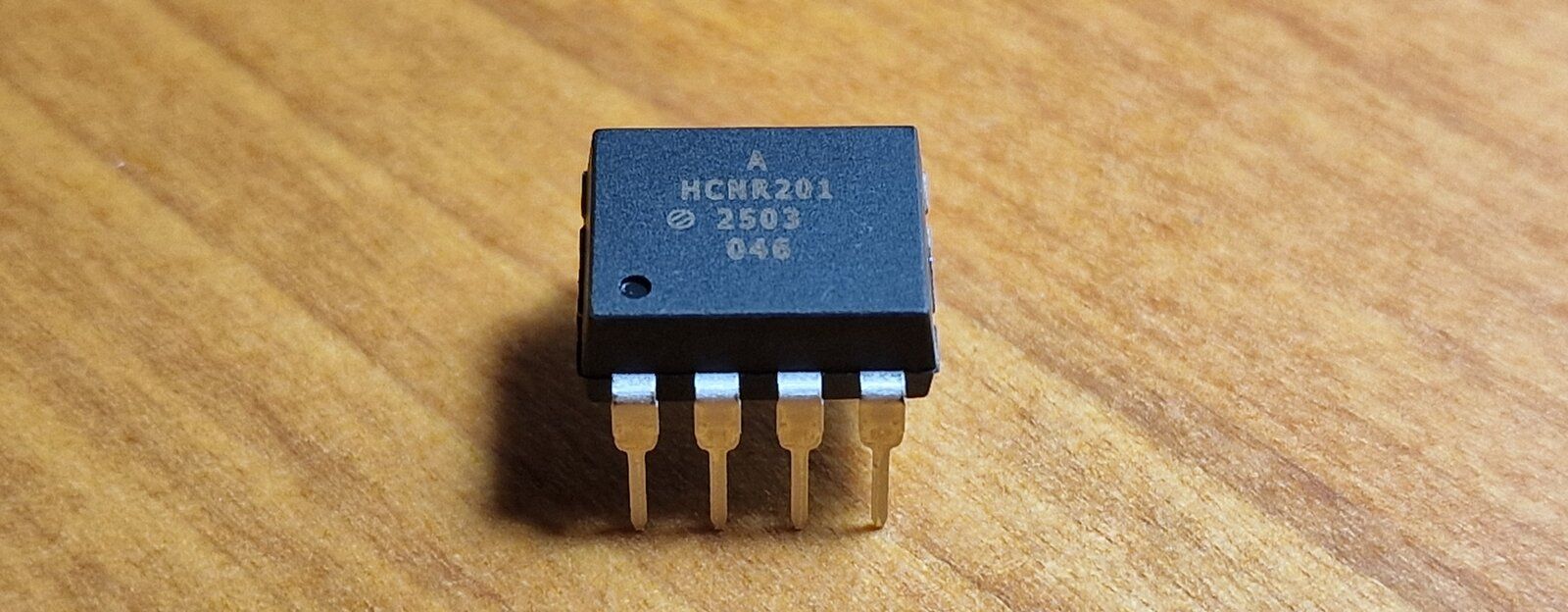
The datasheet of the HCNR201 contains an example circuit that is a good starting point for the design.
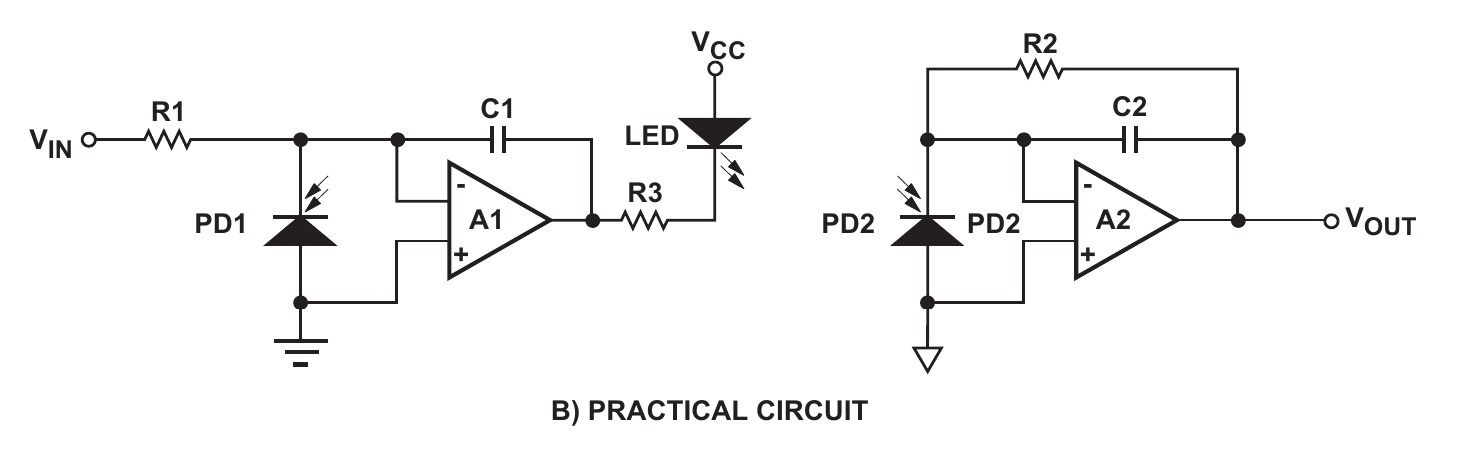
The ratio R_OUT/R_IN is the ideal case; in reality, each device has its own transfer gain K3 = I_PD2/I_PD1, which changes the formula slightly: V_OUT/V_IN = K3 · R_OUT/R_IN.
How the feedback loop works
The HCNR201 contains one LED and two matched photodiodes: PD1 on the input side and PD2 on the output side of the barrier. Both receive light from the same LED.
On the input side, R_IN (R98, 133 kΩ) feeds a current V_IN / R_IN into the inverting input of the op-amp (U14A). PD1 is connected to the same node, and the op-amp drives the LED cathode. If the input current is larger than the PD1 current, the op-amp output goes down, more current flows through the LED (from +3.3 V through R100), the LED gets brighter, and PD1 conducts more. The loop settles when the PD1 current exactly cancels the input current:
I_PD1 = V_IN / R_IN
C97 (1 nF) in the feedback path keeps the loop stable. The important point is that the LED is *inside* the loop. Its efficiency changes with temperature, from part to part and with age, but the op-amp simply drives whatever LED current is needed to keep I_PD1 at V_IN / R_IN. None of these variations reach the output.
On the output side, PD2 sees the same light and produces I_PD2 = K3 · I_PD1. A second op-amp (U13A) works as a transimpedance amplifier: R_OUT (R102 + RV6) in its feedback path turns the photodiode current back into a voltage, V_OUT = I_PD2 · R_OUT. Putting the two sides together gives the formula from above:
V_OUT / V_IN = K3 · R_OUT / R_IN
With 3.3 V at the input and R_IN = 133 kΩ, the full-scale photodiode current is about 25 µA. That is in the middle of the HCNR201 linear range (5 nA to 50 µA), where the datasheet specifies a nonlinearity of 0.05 %. On the output side, R_OUT of roughly 400 to 500 kΩ turns those 25 µA back into the 0–10 V range the high-voltage side expects. The output op-amp is powered from +15 V on the high-voltage side, so no isolated DC/DC converter is needed there.
Since the gain is specific to each part, R_OUT needs to be adjustable over a range that covers the K3 tolerance given in the datasheet.
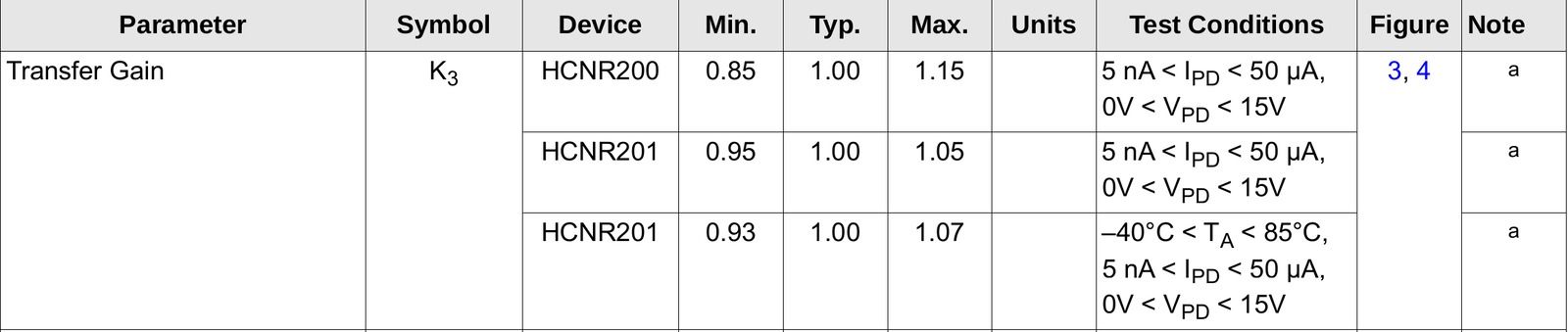
Starting from the datasheet circuit, the practical solution for getting the desired output is to use a potentiometer for R_OUT and calibrate each board.
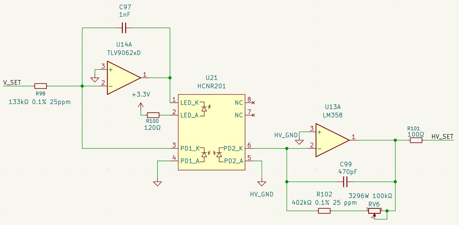
The second part of the analog circuit measures a voltage across the barrier. This works the same way, in the opposite direction. Since op-amps usually come in dual packages, the second op-amp in each package can be used for this channel.
Test PCB
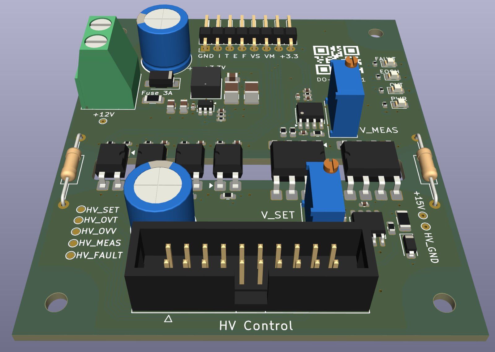
As I mentioned, the board is needed for one of my tests. I designed it in KiCad as a small 4-layer PCB.
For my use case, I also added a small step-down (buck) converter and some LEDs for visual inspection. The two voltage domains are completely separated, and I added a slot in the board to make sure that no contact or short can happen between them. To keep the high-voltage ground close to the low-voltage ground potential, I added a high-resistance connection (10 MΩ) between the two grounds. Strictly speaking, this is a DC path, but the current through it is only in the microamp range, it carries no signal, and it keeps the HV ground from floating to an arbitrary voltage. The signals themselves cross the barrier only through the optocouplers.
The main facts about the board:
| Size | 65 × 75 mm, 1.6 mm FR-4 |
| Layers | 4 (two ground pours, one per domain) |
| Isolation slot | 55 × 5 mm, milled through the board |
| Copper-free gap | the pours stop 2 mm before the slot on each side, on every layer, so there is a 9 mm gap between the two domains |
| Parts across the barrier | 2 × HCNR201 (analog, ≈ 10 mm body creepage per datasheet), 4 × PC817 (digital, 7.62 mm between the pad rows), and the bleed |
| Bleed | 2 × 20 MΩ axial resistors in parallel (10 MΩ), HV_GND to GND |
| Low-voltage side | 12 V input → 3 A fuse → TVS → buck converter → 3.3 V |
| High-voltage side | powered from the +15 V auxiliary output of the device it controls |
| Indicators | PWR, FAULT, OVT and EOCH LEDs on the low-voltage side |
Nothing from one domain runs on any layer under the other one. The inner layers matter as much as the outer ones here: a gap that only exists on the top and bottom is not much use if an inner plane reaches under the other domain. The milled slot helps too. On the surface, creepage has to go around the slot instead of across it.
The narrowest point of the barrier is the PC817 package itself, because its two pad rows are only 7.62 mm apart. If you need more distance, a wide-body optocoupler is the next step. Keep in mind that this is a test board: the spacing is a design target, not a certified isolation rating.
Production at PCBWay and assembly
The board was manufactured by PCBWay as part of a sponsorship, and I think they produced very good-quality PCBs.
For my purpose, I opted for a 4-layer stack-up, which makes routing easy and is affordable for small boards these days. The ordering process was straightforward. A KiCad plugin is available, but I opted for the classic way: export the Gerber and drill files, zip them and upload them on their site. A top/bottom preview of the PCB is shown so you can confirm the overall board before ordering. My suggestion is to always put a serial number or revision on the silkscreen, so you always know which board you are holding. It can help you later :) Production takes a couple of days, and shipping adds a few more days up to one or two weeks, depending on the shipping option.
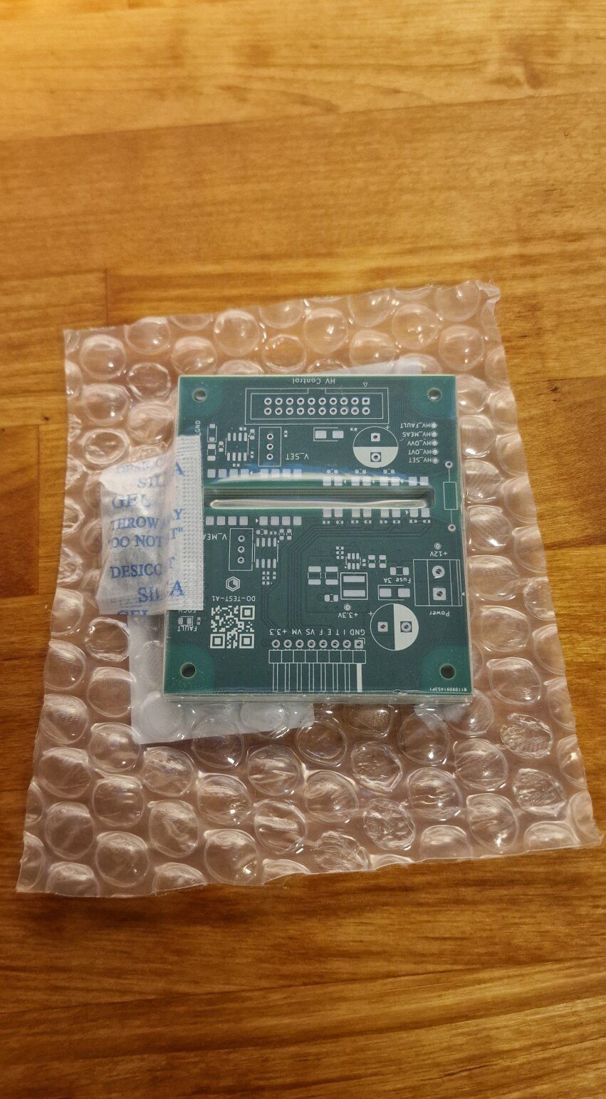
The boards were clean and nicely packed in vacuum-sealed bubble wrap with a desiccant bag.
For the purpose (it is a test board, and I did not want gold plating), the boards look quite nice. The slot that separates the optocoupler sides was perfectly milled, and there were no solder mask, copper or via issues. I particularly like the solder mask: not too glossy, and with a good thickness.
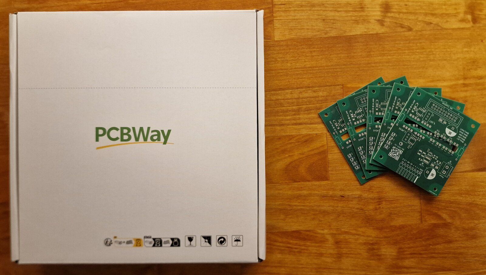
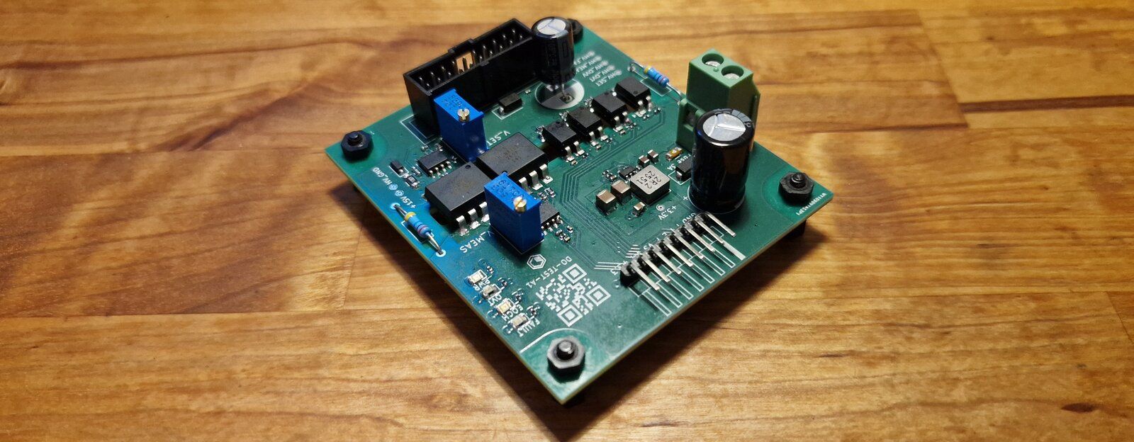
Since I wanted to have the board ready as fast as possible and be able to make my own adjustments along the way, I decided to solder the components myself. What stood out the most was how easy it was to solder, and for that I think the solder mask and the pad clearances matter most.
Often the solder bridges or does not flow properly over the pads, but this time it was really good: everything worked on the first try.
I think good-quality test boards are very important; for development work they are invaluable. Getting them made fast and at a reasonable price is the perfect solution for good and reliable testing and automation. As I mentioned, the goal here is to build a test setup, an automation bench or something very specific that gets the job done reliably. With wires, breadboards and a pile of through-hole components, things get really messy, and you never get your setup tuned and reliable.
Soldering was relatively easy. Some improvements could be made in a second revision, but electrically the board is perfect.
Testing and calibration
With the board soldered, the work is just starting. The first thing to do, always, is to check the power rails for shorts. Once that is safe, check some test points, and only then power the board.
Next, I calibrated the two trimmers and ran a loopback test to confirm that everything works as expected and that the board can be plugged into my test setup.
- Each HCNR201 has its own gain (K3), so each channel gets a trimmer: the one for the setpoint channel is on the HV side, the one for the measurement channel on the LV side.
- The setpoint channel is trimmed under load, with a resistor equal to the input resistance of the controlled device connected.
- The measurement channel is trimmed to a ratio, not to volts. The DAC and the ADC both use VDDA as their reference, so the target is V_ADC / VDDA = 0.72715 with 8.000 V at the input. This is important because the DAC output is proportional to VDDA, while the ADC reading is proportional to 1 / VDDA. It explains why a different 3.3 V source shifts the two channels in opposite directions.
- Loopback: the setpoint output is connected to the measurement input. This checks the whole chain.
For the loopback test, I swept the setpoint from 8 % to 100 % of full scale in 236 steps, 10 times, and compared each reading with the setpoint:
| Readings | 2360 (10 sweeps × 236 steps) |
| Gain error (linear fit) | −0.13 % |
| Readings within one step of the setpoint (1/255 of full scale, ≈ 0.4 %) | 94 % |
| Readings off by 3–5 steps | 0.34 %, single readings that did not repeat at the same setpoint |
The rare outliers came from the wiring of my test setup, not from the board: a few millivolts of voltage drop on the ground wire between the board and the microcontroller board add directly to the measurement. A better cable between the two boards fixed this.
The loopback looks very nice and can be used to validate some of the circuit parameters. Here are some captures I made with the oscilloscope. In both, the yellow line is the input (the setpoint at the microcontroller side) and the blue line is the output (the value measured back). The blue line is shifted up by 0.5 V in the oscilloscope view, only for better visibility.
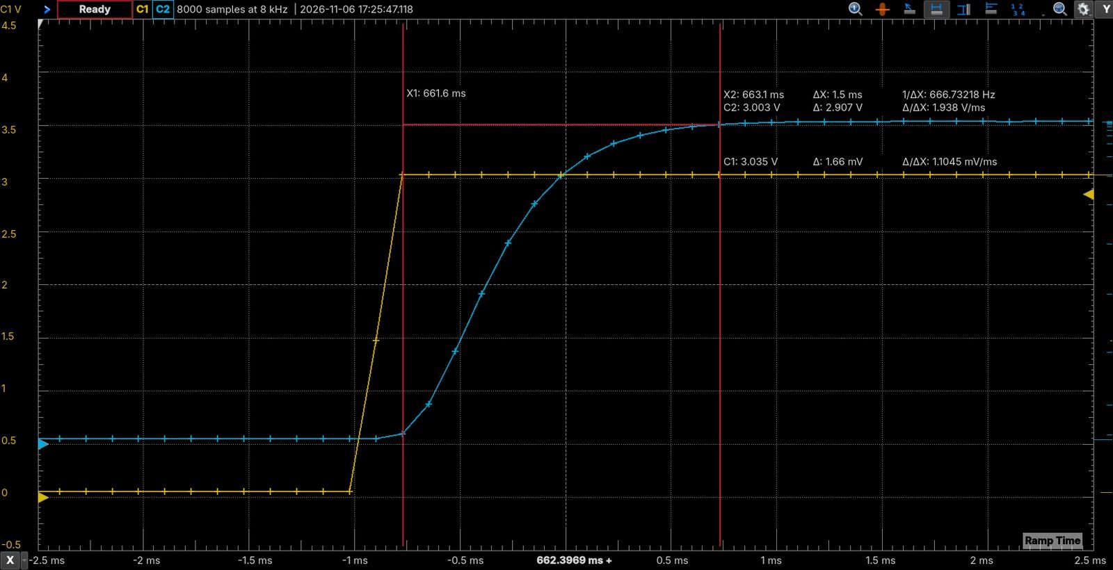
The output settles about 1.5 ms after the input step. This is expected, because in the loopback the signal goes through both channels in series, and each of them is deliberately slow,
Each channel behaves roughly like a low-pass filter with a bandwidth of about 1 kHz. In my simulation, the setpoint channel reaches 90 % in about 0.5 ms and the measurement channel in 0.6–1 ms. Two such stages in series give the S-shaped curve in the capture: a slow start, then an exponential approach to the final value, with no overshoot. That adds up to the 1.5 ms. For setting and reading a slowly changing voltage this is more than fast enough, and the low bandwidth also filters out noise.
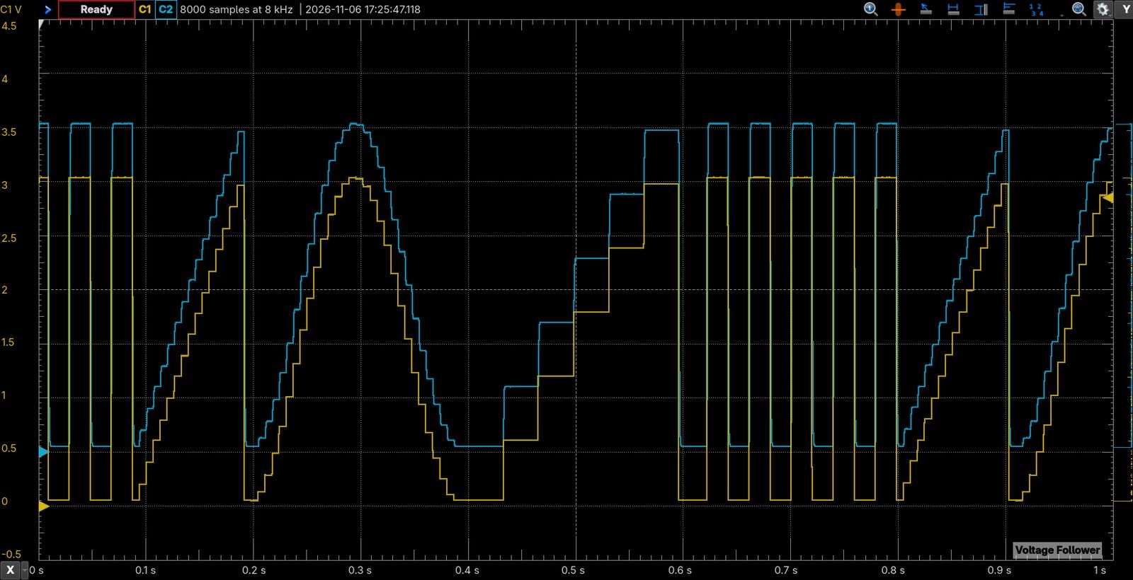
The second capture shows the output following steps, ramps and a square wave over the whole range.
Conclusions
Crossing a voltage barrier with discrete signals is not something you need very often: almost every modern device has a digital interface with a protocol, so you can set a voltage or read a status over a bus. But when a device only offers analog and open-drain signals, or when the two sides must stay completely separated, optocouplers are a simple and practical solution. The PC817 handles the ON/OFF signals with a few resistors, and the HCNR201 in a feedback loop turns an optocoupler into an accurate, linear analog channel, as long as each board is calibrated once. This kind of design knowledge always gives you an edge and can be reused in future projects.
The design files of this small PCB are on GitHub, in case someone needs them, maybe as a starting point for something else: https://github.com/bdmihai/opto-board