The ADC allows a the application to read analog voltages using a single ADC from a maximum of 16 external sources with maximum 12 bit resolution.
Clock (digital part)
Getting the ADC to work on the STM32f411CE requires first a clock. The microcontroller datasheet contains a very intuitive diagram showing the clock tree. The ADC is connected to the APB2 with a maximum 100 MHz. The actual frequency that is uses it depends on the APB prescaler. This will enable the peripheral. The actual GPIO also needs also a clock to be able to function.
    /* confgure the APB clocks */
    MODIFY_REG(RCC->CFGR, RCC_CFGR_PPRE1_Msk, RCC_CFGR_PPRE1_DIV2);
    MODIFY_REG(RCC->CFGR, RCC_CFGR_PPRE2_Msk, RCC_CFGR_PPRE2_DIV2);

    /* enable AHB1 ports clock */
    SET_BIT(RCC->AHB1ENR, RCC_AHB1ENR_GPIOAEN);
    SET_BIT(RCC->AHB1ENR, RCC_AHB1ENR_GPIOBEN);
    SET_BIT(RCC->AHB1ENR, RCC_AHB1ENR_GPIOCEN);
    SET_BIT(RCC->AHB1ENR, RCC_AHB1ENR_GPIOHEN);

    /* enable APB2 devices */
    SET_BIT(RCC->APB2ENR, RCC_APB2ENR_ADC1EN);
Channel
The pin connection is actually defined in the datasheet. There are 16 pins each corresponding to one ADC channel. The decision of what channels are used and in which order the conversion is made is programmable.
    /* set the pis B0 as input ADC */
    MODIFY_REG(GPIOB->MODER, GPIO_MODER_MODER0_Msk, 11);      /* set the pin as analog */
    MODIFY_REG(GPIOB->PUPDR, GPIO_PUPDR_PUPD0_Msk,  0);       /* no pull up, no pull down */

    /* select B0 channel for conversion */
    MODIFY_REG(ADC1->SQR1, ADC_SQR1_L_Msk, 0);
    MODIFY_REG(ADC1->SQR3, ADC_SQR3_SQ1_Msk, 8);
Conversion clock (analog part)
This clock defines the speed of the actual conversion. There is a prescaler that can be configured in order to have a faster/lower conversion speed. This needs to be properly because the actual maximum specified clock lies in the uC datasheet. For example the maximum specified clock for Vdda=3.3V is 36 MHz. By dividing the APB2 Clock (48 MHz) in half (minimum prescaler possible) we get 24 MHz, a value that fulfills the specified maximum.
    /* ADC prescalar 2*/
    MODIFY_REG(ADC1_COMMON->CCR, ADC_CCR_ADCPRE_Msk, 0);
If accuracy/stability is more important, then the clock can be further divided:
    /* ADC prescalar 8 */
    MODIFY_REG(ADC1_COMMON->CCR, ADC_CCR_ADCPRE_Msk, ADC_CCR_ADCPRE_0 | ADC_CCR_ADCPRE_1);
This will give 6 MHz analog clock for the ADC conversion. Another thing is that a normal conversion takes usually 12 clock cycles + channel sampling time.
This is on one side dependent on the ADC resolution as the rate can be increased by decreasing the number of bits. With 12 bit resolution a minimum of 15 (12+3) clock cycles are necessary. If the resolution is reduced to 8 bit then only 11 (8+3) clock cycles are necessary, considering an individual sampling time of 3 cycles.
The channel specific sampling time is individually configurable for each channel and varies from 3 up to 480 cycles. This is programmable and should be defined based on application. More documentation on this can be found in the ST application note AN2834.
    /* select 480 ADC cycles */
    MODIFY_REG(ADC1->SMPR2, ADC_SMPR2_SMP8_Msk, ADC_SMPR2_SMP8_0 | ADC_SMPR2_SMP8_1 | ADC_SMPR2_SMP8_2);
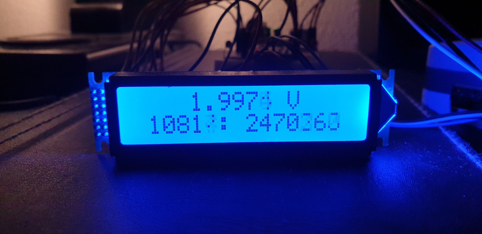
Data read
The data can be pooled or a interrupt can be enabled. Pooling the data is a very fast way to doit but it will block completely the uC.
  /* wait for start of conversion */
  do {
  } while (!(ADC1->SR & ADC_SR_STRT));

  /* wait for end of conversion */
  do {
  } while (!(ADC1->SR & ADC_SR_EOC));
A better option is to enable the end of conversion interrupt and handle each conversion in there. The disadvantage is that the execution of the normal tasks is fragmented by the interrupt triggering quite often (context switch, etc).
    /* 12 bit ADC with interupt enable */
    MODIFY_REG(ADC1->CR1, ADC_CR1_RES_Msk, 0);
    MODIFY_REG(ADC1->CR1, ADC_CR1_EOCIE_Msk, ADC_CR1_EOCIE);

....

void adc_handle_conversion(void)
{
  adc_event_t event;
  event.digital_value = ADC1->DR;
  xQueueSendFromISR(adc_queue, &event, (TickType_t) 0);
}
DMA
The data gathered by the ADC can be stored via DMA directly into memory and processed in a single step. The initialization process is in this case more cumbersome but afterwards there is no more interrupt after each and every conversion. Using double buffering in the DMA makes sense and the entire thing can be send further for processing via the queue events.
    /* configure the pointers/data amount for DMA */
    DMA2_Stream0->PAR  = (uint32_t)&(ADC1->DR);
    DMA2_Stream0->M0AR = (uint32_t)dma_buffer0;
    DMA2_Stream0->M1AR = (uint32_t)dma_buffer1;
    DMA2_Stream0->NDTR = 1000;

    ...

    dma_event_t dma_event;
    dma_event.length = 1000;
    if (DMA2_Stream0->CR & DMA_SxCR_CT_Msk) {
        dma_event.buffer = dma_buffer0;
    } else {
        dma_event.buffer = dma_buffer1;
    }
    xQueueSendFromISR(dma_queue, &dma_event, (TickType_t) 0);
The examples can be found on my github page:
- Simple ADC readout: https://github.com/bdmihai/stm32f411ce-adc
- Read the data in interrupts: https://github.com/bdmihai/stm32f411ce-interrupts
- Scan mode: https://github.com/bdmihai/stm32f411ce-adc-scan
- DMA: https://github.com/bdmihai/stm32f411ce-adc-dma